PCB Manufacturing Process — A Step-by-Step Guide
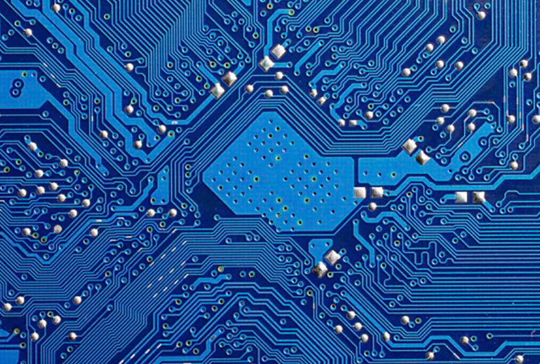
Printed circuit boards (PCBs) form the backbone of all major electronics. These miraculous inventions pop up in nearly all computational electronics, including simpler devices like digital clocks. For the uninitiated, a PCB routes electrical signals through your electronics, which satisfies the device's electrical and mechanical circuit requirements. In short, PCBs tell the electricity where to go, bringing your electronics to life.
PCBs direct current around their surface through a network of copper pathways. The complex system of copper routes determines the unique role of each PCB. At PCBCart we handle the PCB manufacturing process for you from start to finish, but we believe it's important that our clients understand what we do - this ensures that your design specifications better serve your interests. Proper understanding of the PCB manufacturing steps prevents unnecessary errors from getting transmitted during the design stage. It also helps designers stay abreast of the latest printed circuit board manufacturing methods.
In this guide, we'll cover the entire PCB manufacturing process for a standard PCB. From design to completion, and take you through a step-by-step PCB fabrication process.
Basic Anatomy of a PCB Board
Before discussing the PCB manufacturing steps, it's wise to learn about the basic anatomy of a PCB board. The primary component of a PCB is the fiberglass substrate board. The sturdy material provides the strength of the board. We add layers of copper and additional layers of fiberglass substrate and copper onto the substrate, which comprises a typical four layer board. In addition, the PCB board receives a solder mask layer. To employ a biological analogy, consider the fiberglass substrate as the skeleton, the copper layers as the nervous system, carrying electrical signals, and the solder mask layer as the skin, which protects the copper entering into contact with the environment, resulting in a short circuit.
How Is a PCB Manufactured?
Let's examine the full manufacturing process of a PCB — a process that involves 16 steps.
Step 1: Design and Output
It probably comes as no surprise that the first step involves designing the PCB. Technically the first step occurs in the mind of the designer, but we'll skip that part. Like all manufactured goods, PCB relies on a plan. Depending on the PCB requirements, the designer creates a layout using industry standard design software.
The most frequently used program is called extended Gerber. The 1980's baby food ad campaign sought beautiful babies, and this software creates some beautifully designed offspring. Gerber also goes by the name IX274X. The PCB industry birthed extended Gerber as the perfect output format. The software encodes all vital information — the copper tracking layers, component notations, and the solder masks. All aspects of the PCB design undergo checks at this point. The software performs oversight algorithms on the design to ensure that no errors go undetected. The designer also examines the plan with regard for elements relating to track width, board edge spacing, trace and hole spacing and hole size.
After a thorough examination, the designer outputs the PCB design to the fabrication house for them to build. Once received, the PCB fabricator performs a check, called a Design for Manufacture (DFM) check, to ensure the design will fulfill requirements for the minimum tolerances during the manufacturing process.
Step 2: From File to Film
After the designer outputs the PCB schematic files and the manufacturer conducts a DMF check, it's time to print. PCB files don't print to a regular printer. The manufacturer uses a special printer called a plotter, which makes photo films of the PCBs. The manufacturer will use the films to image the PCBs. Although they're laser printers, they aren't a standard laser jet printer. Plotters use incredibly precise printing technology to provide a highly detailed film of the PCB design.
The manufacturer also controls the temperature and humidity of the printing environment to mitigate any outside influences in printing the film, which resembles the transparencies used to project images on a screen. Depending on your age, you might remember them from high school. Sheets of clear plastic enter the plotter and receive the PCB design in black ink. The final product results in a plastic sheet with a photo negative of the PCB in black ink. For the inner layers of the PCB, black ink represents the conductive copper parts of the PCB. The remaining clear portion of the image denotes the areas of non-conductive material. The outer layers follow the opposite pattern: clear for copper, but black refers to the area where the manufacturer will remove existing copper. The plotter automatically develops the film, and the film is securely stored to prevent any unwanted contact.
Each layer of PCB and solder mask receive their own clear and black film sheet. In total, a two-layer PCB needs four sheets: two for the layers and two for the solder mask. Of course, the films correspond perfectly to each other. When used in harmony, they map out the PCB alignment.
An exact overlapping of the films is achieved when the technician punches a hole through all the films. The registration hole serves as an alignment guide. The exactness of the hole occurs by adjusting the table on which the film sits. When the tiny calibrations of the table lead to an optimal match, the hole is punched. The holes will fit into the registration pins in the next step of the imaging process.
Step 3: Printing the Inner layers: Where Will the Copper Go?
This step in PCB manufacture prepares to make actual PCB. The basic form of PCB comprises a laminate board. Laminate serves as an ideal body for receiving the copper that structures the PCB. The epoxy resin and glass fiber core of the laminate sheet provides a sturdy and dust-resistant starting point for the PCB. Copper is pre-bonded on both sides. The process involves whittling away the copper to reveal the design from the films.
In PCB construction, cleanliness is key. The copper-sided laminate is cleaned and passed into a decontaminated environment. During this stage, it's vital that no dust particles settle on the laminate. An errant speck of dirt might otherwise cause a circuit to short or remain open.
Next, the clean panel receives a layer of photo-sensitive film called the photo resist. The photo resist comprises a layer of photo reactive chemicals that harden after exposure to ultra violet light. This ensures an exact match from the photo films to the photo resist. The films fit onto pins that hold them in place over the laminate panel.
The film and board line up and receive a blast of UV light. The light passes through the clear parts of the film, hardening the photo resist on the copper underneath. The black ink from the plotter prevents the light from reaching the areas not meant to harden, and they are slated for removal. The aspect of light control is vital during this stage, and only yellow light floods the interior of the room. Yellow light carries the least UV level wavelengths.
After the board becomes prepared, it is washed with an alkaline solution that removes any photo resist left unhardened. A final pressure wash removes anything else left on the surface. The board is then dried.
The product emerges with resist properly covering the copper areas meant to remain in the final form. A technician examines the boards to ensure that no errors occurred during this stage. All the resist present at this point denotes the copper that will emerge in the final PCB.
This step only applies to boards with more than two layers. Simple two-layer boards skip ahead to drilling. Multiple-layer boards require more steps.
Step 4: Removing the Unwanted Copper
With the photo resist removed and the hardened resist covering the copper we wish to keep, the board proceeds to the next stage: unwanted copper removal. Just as the alkaline solution removed the resist, a more powerful chemical preparation eats away the excess copper. The copper solvent solution bath removes all of the exposed copper. Meanwhile, the desired copper remains fully protected beneath the hardened layer of photo resist.
Not all copper boards are created equal. Some heavier boards require larger amounts of copper solvent and varying lengths of exposure. As a side note, heavier copper boards require additional attention for track spacing. Most standard PCBs rely on similar specification.
Now that the solvent removed the unwanted copper, the hardened resist protecting the preferred copper needs washing off. Another solvent accomplishes this task. The board now glistens with only the copper substrate necessary for the PCB.
Step 5: Layer Alignment and Optical Inspection
With all the layers clean and ready, the layers require alignment punches to ensure they all line up. The registration holes align the inner layers to the outer ones. The technician places the layers into a machine called the optical punch, which permits an exact correspondence so the registration holes are punched perfectly.
Once the layers are placed together, it's impossible to correct any errors on the inner layers. Another machine performs an automatic optical inspection of the panels to confirm a total absence of defects. The original design from Gerber, which the manufacturer received, serves as the model. The machine scans the layers using a laser sensor and proceeds to electronically compare the digital image with the original Gerber file.
If the machine finds an inconsistency, the comparison is displayed on a monitor for the technician to assess. Once the layer passes inspection, it moves to the final stages of PCB production.
Step 6: Lay-up and Bond
In this stage, the PCB takes shape. All the separate layers await their union. With the layers ready and confirmed, they simply need to fuse together. Outer layers must join with the substrate. The process happens in two steps: lay-up and bonding.
The outer layer material consists of sheets of fiber glass, pre-impregnated with epoxy resin. The shorthand for this is called prepreg. A thin copper foil also covers the top and bottom of the original substrate, which contains the copper trace etchings. Now, it's time to sandwich them together.
The bonding occurs on a heavy steel table with metal clamps. The layers securely fit into pins attached to the table. Everything must fit snugly to prevent shifting during the alignment.
A technician begins by placing a prepreg layer over alignment basin. The substrate layer fits over the prepreg before the copper sheet is placed. Further sheets of prepreg sit on top of the copper layer. Finally, an aluminum foil and copper press plate complete the stack. Now it's prepped for pressing.
The technician slides the stack over to the mechanical press, which compresses the layers. Then, pins are driven through the stack to ensure its fixation together. Next, the stack is placed on a tray and taken to the bonding press.
The bonding press employs heat controlled plates to apply pressure to the stack. The heat in the press melts the epoxy resin while the press applies pressure to fuse the stack together. The entire operation undergoes an automatic routine run by the bonding press computer. The computer orchestrates the process of heating up the stack, the point in which to apply pressure, and when to allow the stack to cool at a controlled rate.
Next, a certain amount of unpacking occurs. With all the layers molded together in a super sandwich of PCB glory, the technician simply unpacks the multi-layer PCB product. It's a simple matter of removing the restraining pins and discarding the top pressure plate. The PCB goodness emerges victorious from within its shell of aluminum press plates. The copper foil, included in the process, remains to comprise the outer layers of the PCB.
Step 7: Drill
Finally, holes are bored into the stack board. All components slated to come later, such as copper-linking via holes and leaded aspects, rely on the exactness of precision drill holes. The holes are drilled to a hairs-width-the drill achieves 100 microns in diameter, while hair averages at 150 microns.
To find the location of the drill targets, an x-ray locator identifies the proper drill target spots. Then, proper registration holes are bored to secure the stack for the series of more specific holes.
Before drilling, the technician places a board of buffer material beneath the drill target to ensure a clean bore is enacted. If you've ever used a home drill and placed a piece of scrap wood below your drill site to eliminate splintering, it's the same idea. The exit-material prevents any unnecessary tearing upon the drill's exits.
A computer controls every micro-movement of the drill — it's only natural that a product that determines the behavior of machines would rely on computers. The computer-driven machine uses the drilling file from the original design to identify the proper spots to bore.
The drills use air-driven spindles that turn at 150, 000 rpm. At this speed, you might think that drilling happens in a flash, but there are many holes to bore. An average PCB contains well over one hundred bore intact points. During drilling, each needs its own special moment with the drill, so it takes time. The holes later house the vias and mechanical mounting holes for the PCB. The final affixation of these parts occurs later, after plating. After the drilling completes itself, the additional copper that lines the edges of the production panel undergoes removal by a profiling tool.
Step 8: Plating and Copper Deposition
After drilling, the panel moves onto plating. The process fuses the different layers together using chemical deposition. After a thorough cleaning, the panel undergoes a series of chemical baths. During the baths, a chemical deposition process deposits a thin layer — about one micron thick — of copper over the surface of the panel. The copper goes into the recently drilled holes.
Prior to this step, the interior surface of the holes simply exposes the fiber glass material that comprises the interior of the panel. The copper baths completely cover, or plate, the walls of the holes. Incidentally, the entire panel receives a new layer of copper. Most importantly, the new holes are covered. Computers control the entire process of dipping, removal and procession.
Step 9: Outer Layer Imaging
In Step 3, we applied photo resist to the panel. In this step, we do it again — except this time, we image the outer layers of the panel with the PCB design. We begin with the layers in a sterile room to prevent any contaminants from sticking to the layer surface. We apply a layer of photo resist to the panel. The prepped panel then passes into the yellow room. UV lights affect photo resist. Yellow light wavelengths don't carry UV levels sufficient to affect the photo resist.
Black ink transparencies are secured by pins to prevent misalignment with the panel. With panel and stencil in contact, a generator blasts them with high UV light, which hardens the photo resist. The panel then passes into a machine that removes the unhardened resist, protected by the black ink opacity.
The process stands as an inversion to that of the inner layers. Finally, the outer plates undergo inspection to ensure all of the undesired photo resist was removed during the previous stage.
Step 10: Plating
We return to the plating room. As we did in step 8, we electroplate the panel with a thin layer of copper. The exposed sections of the panel from the outer layer photo resist stage receive the copper electro-plating. Following the initial copper plating baths, the panel usually receives tin plating, which permits the removal of all the copper left on the board slated for removal. The tin guards the section of the panel meant to remain covered with copper during the next etching stage. Etching removes the unwanted copper foil from the panel.
Step 11: Final Etching
The tin protects the desired copper during this stage. The unwanted exposed copper and copper beneath the remaining resist layer undergo removal. Again, chemical solutions are applied to remove the excess copper. Meanwhile, the tin protects the valued copper during this stage.
The conducting areas and connections are now properly established.
Step 12: Solder Mask Application
Before the solder mask is applied to both sides of the board, the panels are cleaned and covered with an epoxy solder mask ink. The boards receive a blast of UV light, which passes through a solder mask photo film. The covered portions remain unhardened and will undergo removal.
Finally, the board passes into an oven to cure the solder mask.
Step 13: Surface Finish
To add extra solder-ability to the PCB, we chemically plate them with gold or silver. Some PCBs also receive hot air-leveled pads during this stage. The hot air leveling results in uniform pads.
Step 14: Silkscreen
The nearly completed board receives ink-jet writing on its surface, used to indicate all vital information pertaining to the PCB. The PCB finally passes onto the last coating and curing stage.
Step 15: Electrical Test
As a final precaution, a technician performs electrical tests on the PCB. The automated procedure confirms the functionality of the PCB and its conformity to the original design. At PCBCart, we offer an advanced version of electrical testing called Flying Probe Testing. This testing depends on moving probes to test electrical performance of each net on a bare circuit board.
Step 16: Profiling and V-Scoring
Now we've come to last step: cutting. The different boards are cut from the original panel. The method employed either centers on using a router or a v-groove. A router leaves small tabs along the board edges while the v-groove cuts diagonal channels along both sides of the board. Both ways permit the boards to easily pop out from the panel.
What to Look For in a PCB Manufacturer
As you can see, a lot of work goes into the PCB fabrication process. At PCBCart, we are always focused on the care and attention to detail that each PCB manufacturing step requires. We also offer vacuum packaging, weighing and delivery to make sure your PCB order arrives safely and free of damage.
When picking a PCB manufacturer, be sure to choose a company with a high level of expertise and a focus on quality at each stage. Our knowledge, consideration and technical ability shows in every part of our work.
If you are interested in learning more, check out our PCB Fabrication or Assembly sections. We offer fast turnaround and free PCB quotes.
Source : https://www.pcbcart.com/article/content/PCB-manufacturing-process.html/
Related Posts
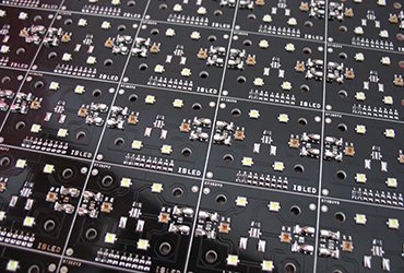
Metal Core PCB means the core (base) material for PCB is the metal, not the normal FR4/CEM1-3, etc. and currently the most common metal used for MCPCB manufacturer are Aluminum, Copper and steel alloy. Aluminum has good heat transferring and dissipation ability, but yet relatively cheaper; copper has even better performance but relatively more expensive, and steel can be divided into normal steel and stainless steel. It more rigid than both aluminum and copper, but thermal conductivity is lower than them too. People will choose their own base/core material according to their different application....
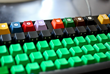
There are many ranges of keyboards from many different makers out there, most of whom are either membrane keyboards or mechanical keyboards. Being a gamer and a typist I used many different keyboards over the years, all with their different benefits or downfalls. Some feel good on my hands, others not so. When you do a lot of work or a lot of gaming, you want something that will perform well to your fingers. Now not all keyboards are made the same granted that some are made better than others even if they are similar. Today we will compare the membrane keyboard and mechanical keyboard, and provide recommendations about who should use membrane keyboard and who should use mechanical keyboard....